NanoArt Competition
2022 Winners
Nanoboomerang Forest
Most Unique Capability
Artists: Shawn Wimer (Graduate
Student), Dr. Ufuk Kilic, and Dr. Matthew Hilfiker
Tool: FEI Helios NanoLab 660 and FEI Tecnai Osiris (S)TEM
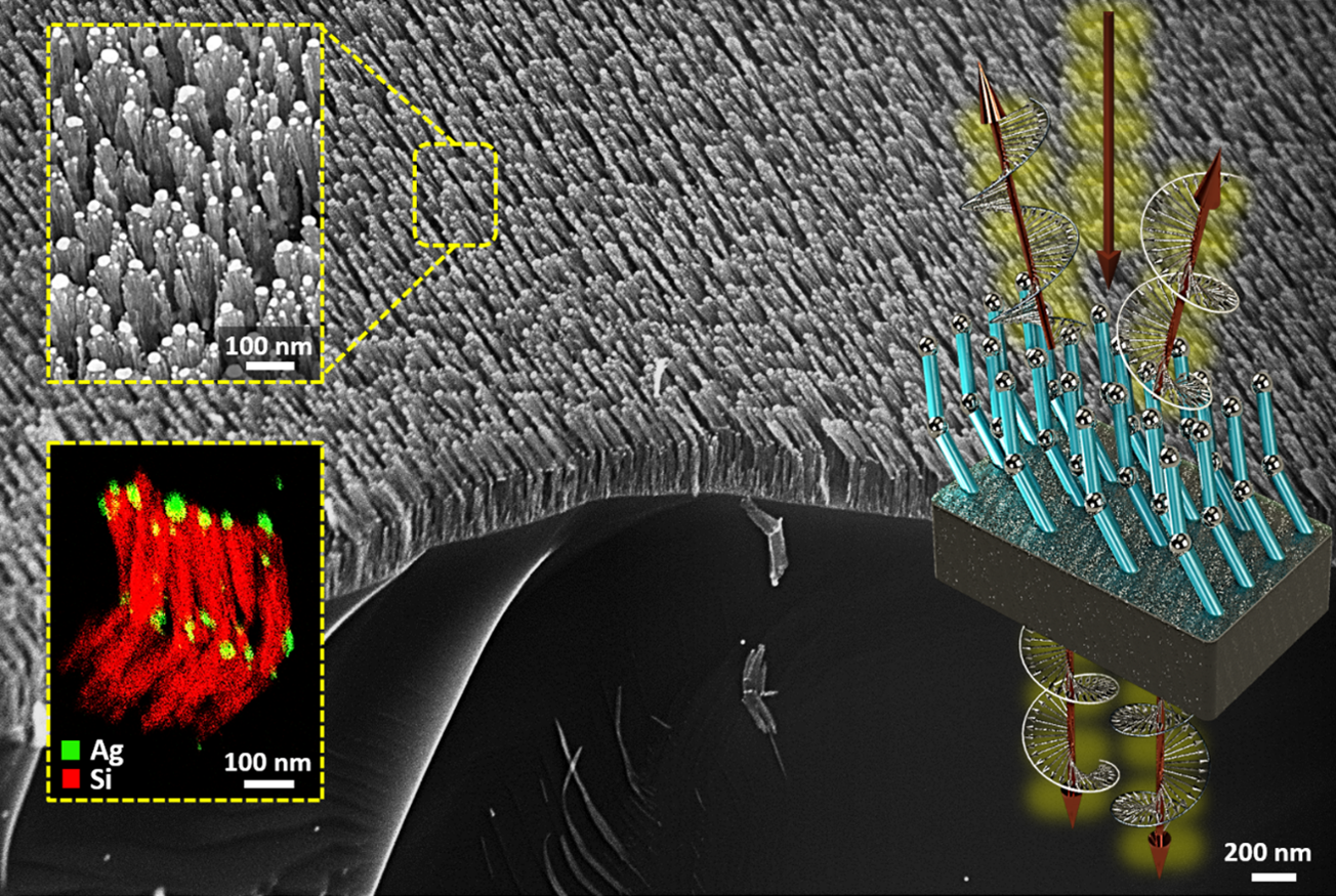
Recently, there has been a paradigm shift in the engineering of optical materials from single material building blocks to the hybridized metamaterial platforms which can unlock new possibilities in the manipulation of chiral light-matter interactions at nano scale. This collage image shows our new metamaterial design: wafer-scale-area deposited, spatially coherent, super-lattice type, three-dimensional, distorted L-shape plasmonic hybrid metamaterial so-called plasmonic Nanoboomerang. Here, the scanning electron microscope image (SEM) from the tilted cross section of the sample was shown with the top view SEM image and the Scanning-Transmission-Electron-Microscopy image with atomic resolution energy-dispersive X-ray spectroscopy-based material mapping as insets.
Helical Metamaterial Platform
Most Stunning
by Shawn Wimer (Graduate Student), Dr.
Ufuk Kilic, and Dr. Matthew Hilfiker
Tool: FEI Tecnai Osiris (S)TEM
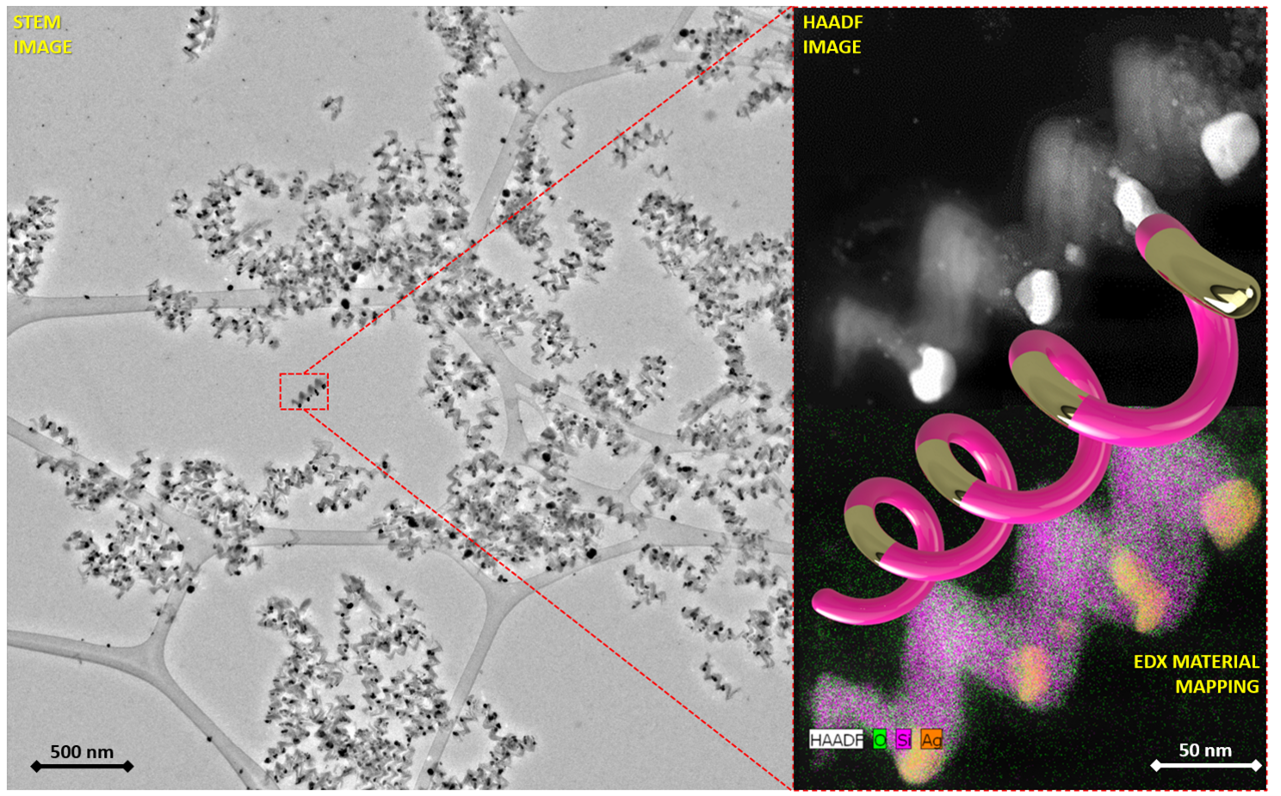
Here, the highly porous, super-lattice type, periodic arrangements of nano-plasmonic, right-handed Silicon (Si)-Silver(Ag) chiral heterostructure metamaterial platform were fabricated by means of subsequent and repeated electron-beam glancing angle deposition from Si and Ag sources. The figure collage shows the scanning transmission electron microscopy (STEM) image which enabled a prominent ability to create contrast and distinguish Si and Ag sub-helical segments (left image), the high-angle-annular-dark-field STEM enabled to focus on isolated single helicaL heterostructure system (right top image) and the atomic resolution energy-dispersive X-ray spectroscopy-based material mapping enables to map the material along single Si-Ag helical heterostruture metamaterial (right bottom image).
Sandhill Crane
Most Whimsical
Artist: Shawn Wimer (PhD student) and
Ufuk Kilic (post doc)
Tool: FEI Tecnai Osiris (S)TEM
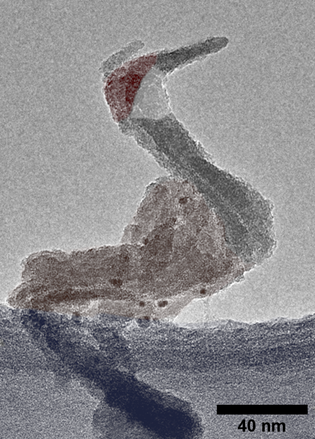
This image is of a helical silicon nanostructure and a bit of extra broken material from another structure hanging from the carbon nanofilm of a TEM grid. The nanostructures are deposited as a dense film, usually 100-300 nm thick, and have optical applications related to the change in polarization of incident and transmitted light.
2021 Winners
Butterfly
Most Unique Capability
Artists: A.A. Kovalev and Bo Li
Tool: mumax3 micromagnetic simulator and Wolfram Mathematica
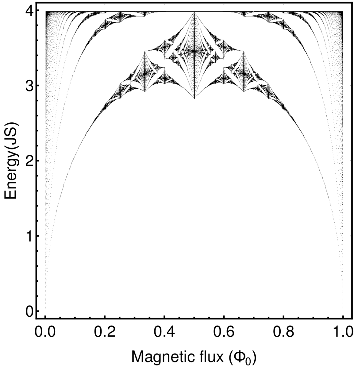
The image represents Hofstadter’s butterfly describing magnons -- excitations in a small sample made of an antiferromagnet. The horizontal axis corresponds to the strength of spin-orbit interaction gradient while the vertical axis corresponds to energy. Due to the presence of magnetic field the picture reveals fractal, self-similar pattern. Surprisingly, rather than revealing the typical Hofstadter’s butterfly corresponding to electrons, antiferromagnetic magnons reveal Hofstadter’s butterfly corresponding to Klein-Gordon equation typically used in high-energy physics.
A Micro Blooming Lotus
Most Stunning - NNCI Winner
by Aofei Mao and Peixun Fan
Tool: Nanoscribe Photonic Professional GT and Hitachi S4700 field emission scanning electron
microscope
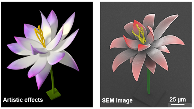
When engineers become artists, a micro blooming lotus with a dimension smaller than the diameter of human hair was created via a microscale 3D printing technology: two-photon polymerization (Nanoscribe Photonic Professional GT). To make sure the over-hang features of this tiny lotus could survive, Ph.D. student Aofei Mao, Dr. Peixun Fan, and Prof. Yongfeng Lu from the Laser Assisted Nano-Engineering Lab invented their “gradient polymerization” technique by finely controlling the printing parameters. The sample was sputtering-coated for SEM imaging using a Hitachi S4700 field emission scanning electron microscope.
Rocky Marshland
Most Whimsical
Artist: Oghenetega Allen Obewhere
Tool: Anasys afm+ AFM
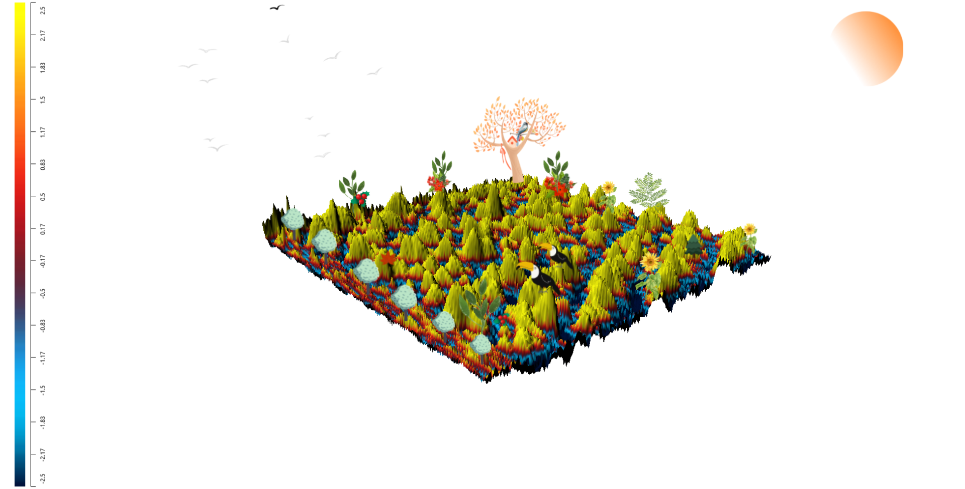
A 3-D contact resonance atomic force microscopy (CR-AFM) phase image of thin-film ion-conducting polymer (Nafion) and Platinum nanoparticles (Pt-NPs). Ion conducting polymers play a crucial role as binders on the electrode surface of electrochemical devices where they help to fix the catalysts to the electrode surface. An optimized ratio of catalyst/ionomer is needed for the efficient electrochemical reactions at the electrodes of these devices. This CR-AFM surface image elucidates the extent of nanoparticles dispersion within the ionomer film (Nafion, blue and Pt-NPs, green) at this loading and it has been recreated as a rocky coastal marshland in the dark.
2020 Winners
| Most Stunning
NNCI Honorable Mention by: Kossi Loic M Avegnon 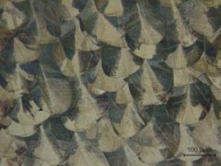
"Optical Microscopy of 316 stainless steel additively manufactured" Department of Mechanical & Materials Engineering |
Most Unique Capability by: Zahra Ahmadi 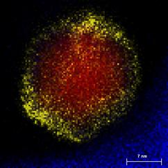
"The Sunset" Department of Mechanical & Materials Engineering |
Most Whimsical by: Seefat Farzin and Mohammad Mazharul Islam 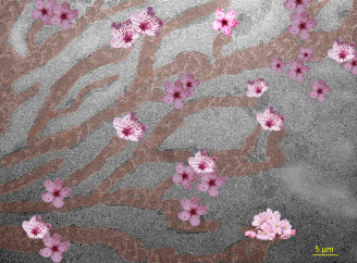
"Sakura on TEM Grid" Department of Chemical and Biomolecular Engineering |
2019 Winners
by Loic Constantin
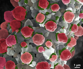
"The Copper Garden"
by Ufuk Kilic and Mathew Hilfiker
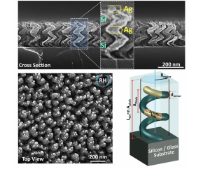
"SiAg Chiral nanoplasmonic metasurfaces"
by Seefat Farzin and Mohammad Mazharul Islam
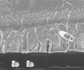
"Happiness Comes in Waves"
2016
1st place
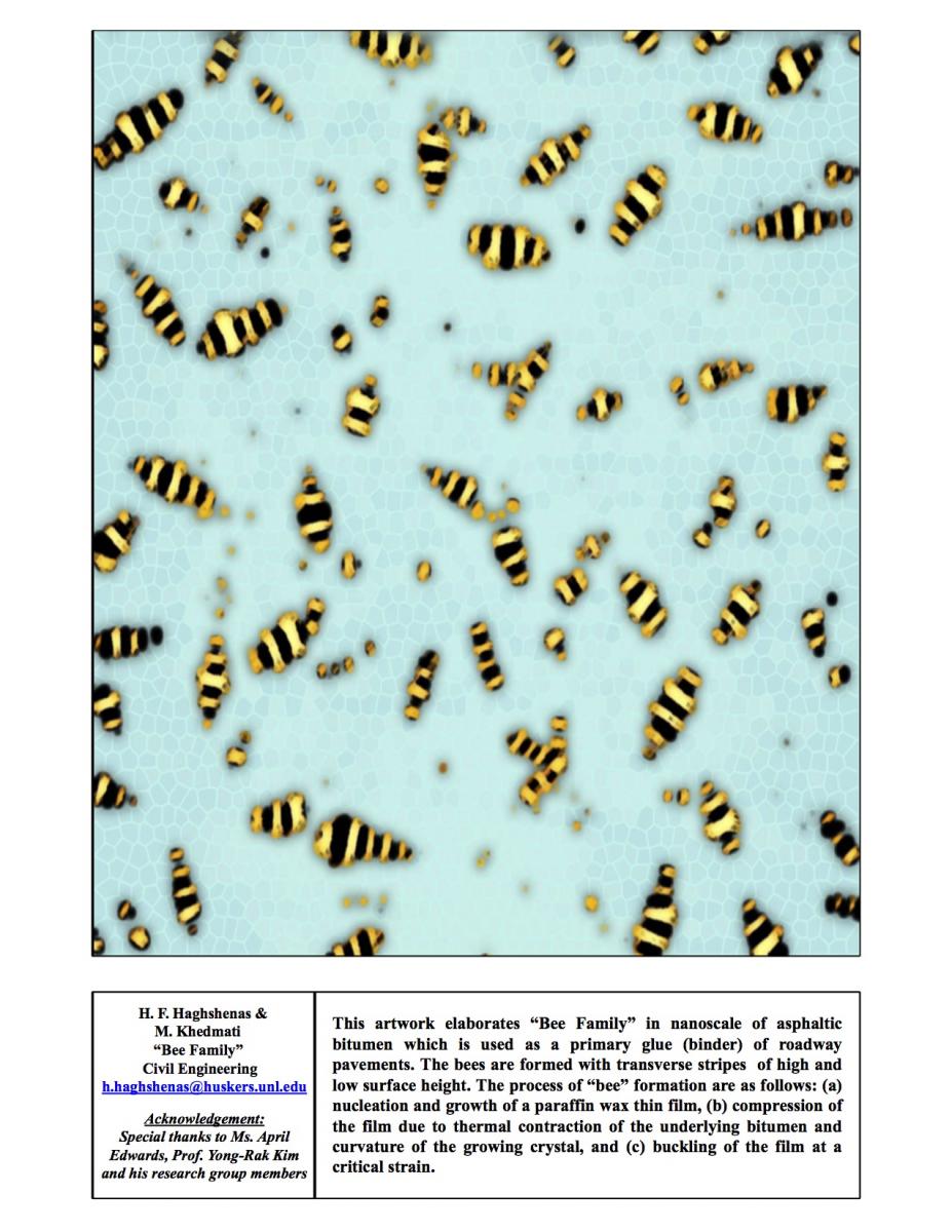
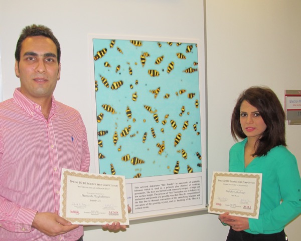
H. F. Haghshenas & M. Khedmati
"Bee Family"
2nd place
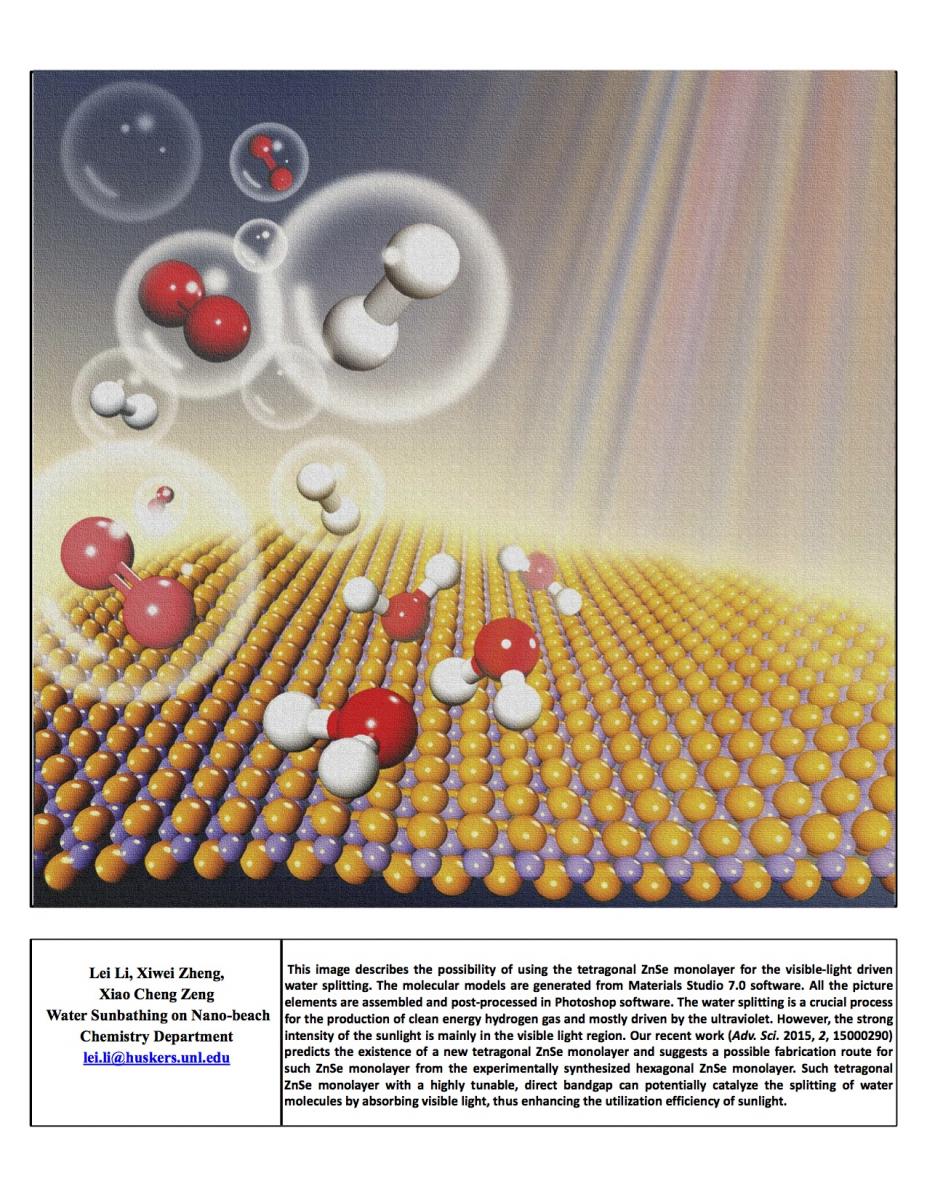
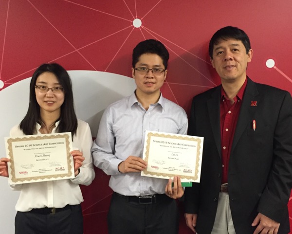
Lei Li, Xiwei Zheng, Xiao Cheng Zeng
"Water Sunbathing on Nano-beach"
2014-15
