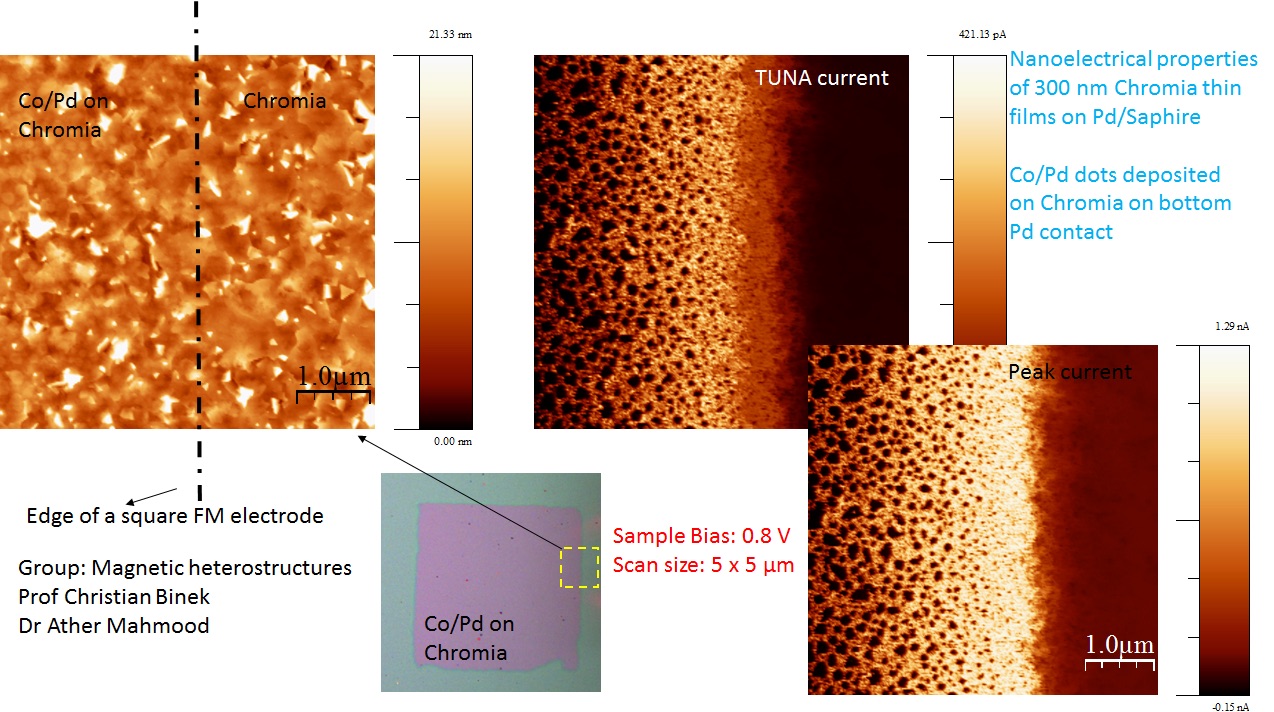
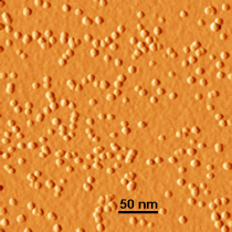
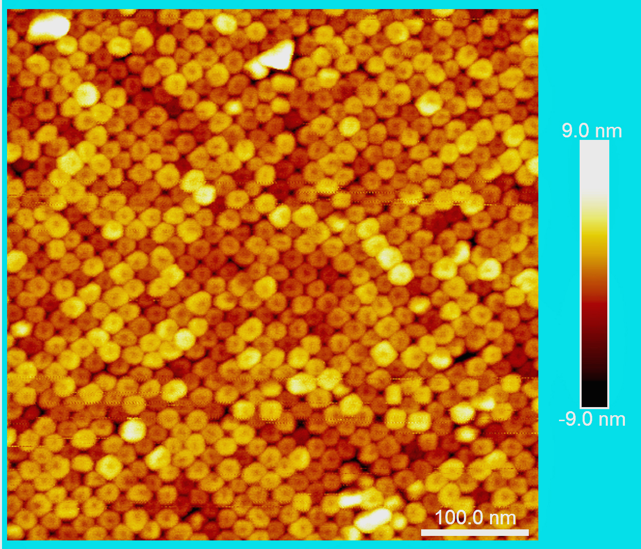
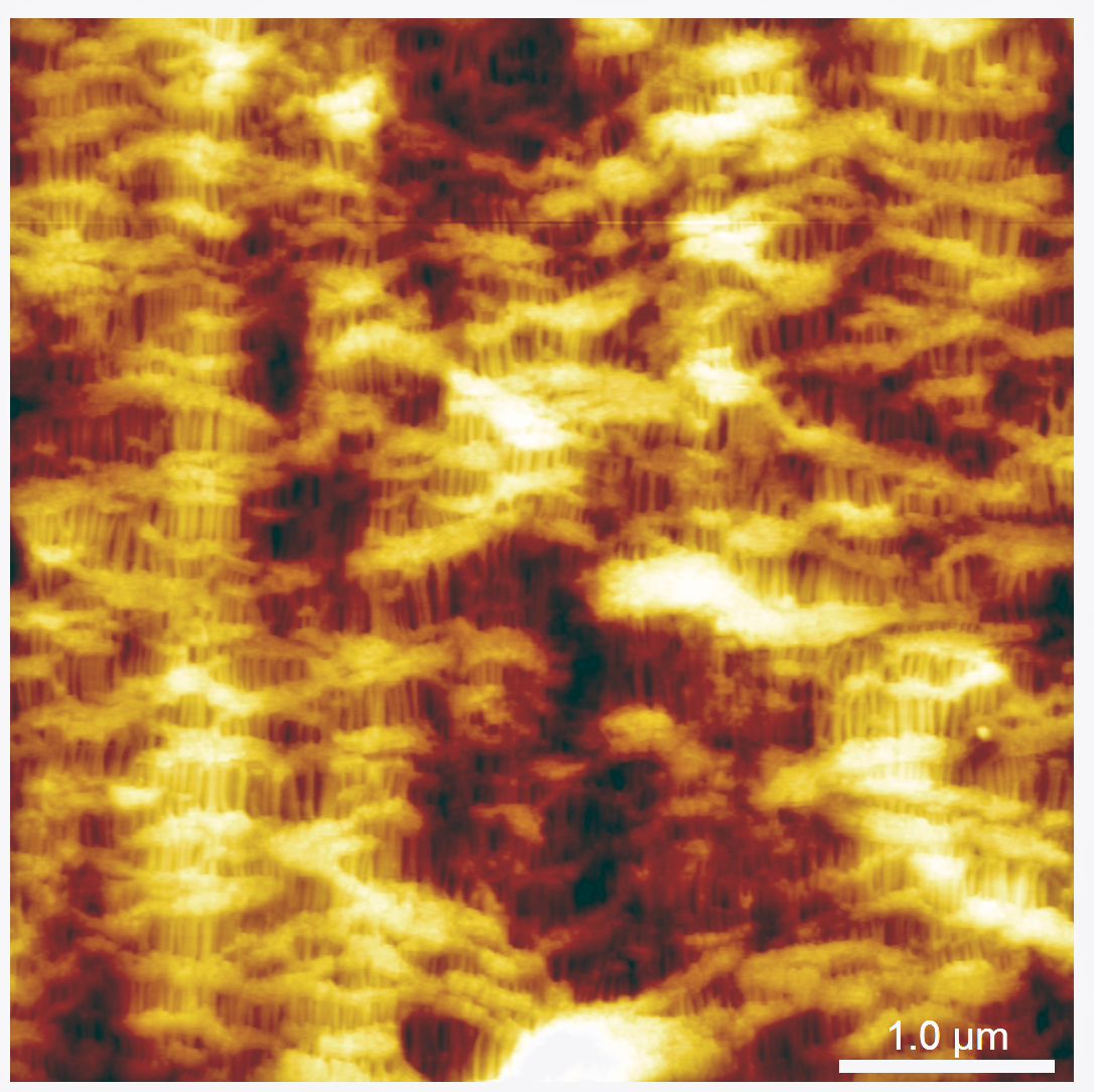
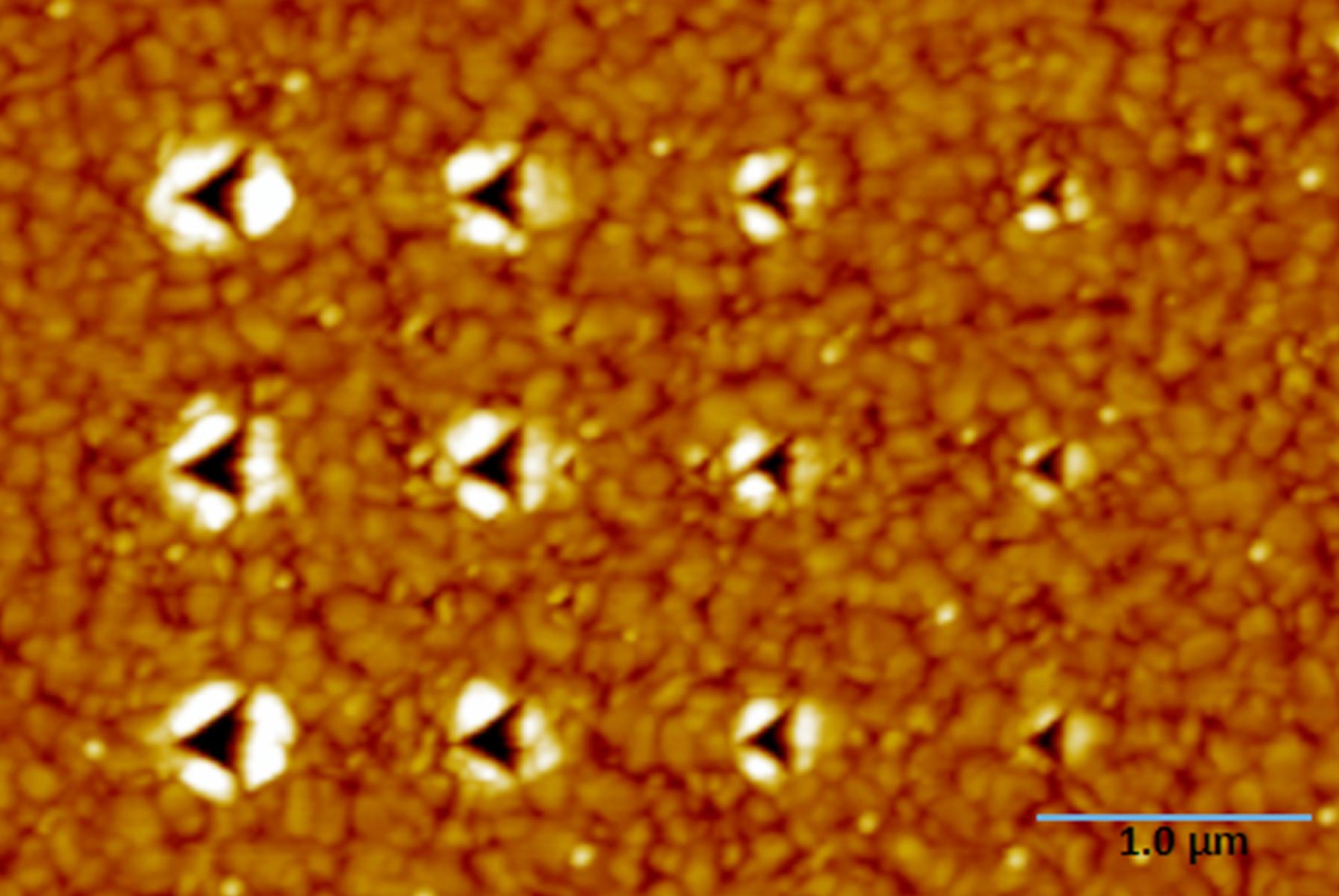
Topographic and current images of Co/Pd dots deposited on Chromia sample using PeakForce TUNA. Image courtesy of Dr. Mahmood, Prof. Binek, UNL. (click to enlarge)10 x 10 µm topographic image of a virgin asphat binder show the beelike structure. Sample provided by Hamzeh Haghshenas, Prof. Kim, UNL.Polyhydroxyaalkanoates (PHAs) crystallization picture captured by Olympus BX51 microscope. A hot stage is used to melt PHA, and is then slowly cooled to obtain a crystalline structure. Picture courtesy of Ehsan Rezaei, UNL.AFM image of monodispersed, sub-10nm Fe clusters produced by inert gas condensationMFM domain images of Co/Pt multi-layers with 8, 10.5, 11, and 12 Å NiO interlayers. Image courtesy of Dr. Baruth, Prof. Adenwalla, UNL.AFM image of the as-synthesized Co. Sample courtesy of Yongsheng Yu.
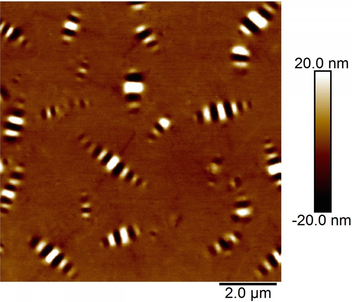
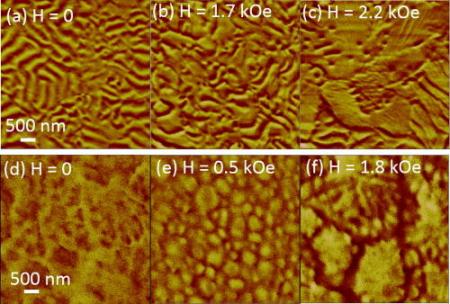
MFM images measured at various field for NiMnGa (a-c) and NiMnIn (d-f).
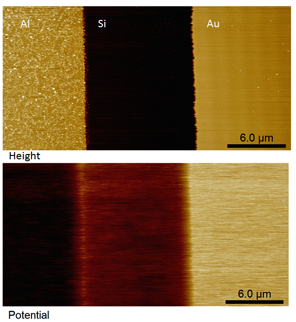
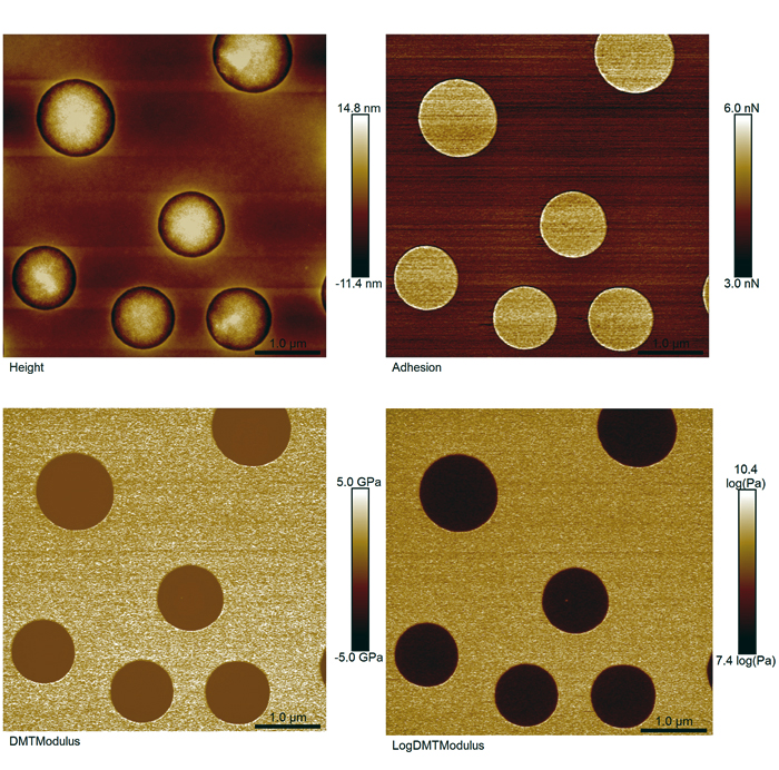
Appl. Phys. Lett. 115, 172404 (2019); DOI: 10.1063/1.5120406Height (top) and potential (bottom) images using PeakForce KPFM on a Au- Si-Al strips sample. Both the Al and Au films are 50 nm in thickness deposited on an n-doped silicon substrate.Height image of a PS+LDPE blend sample with respective adhesion and modulus maps.Fluid AFM using ScanAsyst mode on celgard sampleNanoindentation on a gold thin film using four different forces of about 50, 40, 30, and 20 µN respectively with three indents made at each force.Nanomanipulation