Overview
The Surface and Materials Characterization (SMCF) Central Facility is operated by the Nebraska Center for Materials and Nanoscience (NCMN). This facility is open to all University of Nebraska-Lincoln researchers as well as external users with well-defined user fees. The SMCF central facility is located in the basement of Jorgensen Hall (Room 013, 011, and 009) at the University of Nebraska-Lincoln.
The facility specialist, Dr. Lanping Yue (see Contact Info) is in charge of the SMCF central facility to maintain equipment, train and assist users. Research collaborations are welcome from all university research groups as well as companies in Nebraska and elsewhere.
The SMCF facility provides state-of-the-art instruments for nanometer-scale characterization of materials surface and related physical properties. The SMCF specializes in scanning probe microscopies (SPM) such as Atomic Force Microscopy (AFM), Magnetic Force Microscopy (MFM), Electrostatic Force Microscopy (EFM), Scanning Tunneling Microscopy (STM), Piezoresponse Microscopy (PFM), Surface Potential Microscopy (PeakForce KPFM), PeakForce Tunneling AFM (PF-TUNA) and Quantitative Nanomechanical Property Mapping (PF-QNM), etc. These SPM instruments have the ability to operate in ambient air, vacuum, liquids, and different temperature environment. AFM can provide three-dimensional high contrast topographic images with sub-nanometer resolution including line width, grain size, thin film thickness, roughness measurements, sectioning of surfaces, particle analysis, surface defects, and pattern recognition, etc. Depending on the interaction of scanning probe and sample surface, a variety of physical properties can be measured such as electrical, magnetic, and nanomechanical properties.
In addition to the SPM systems, the Facility also offers non-probe based equipment for measuring thermal properties; a Differential Scanning Calorimeter (DSC), a Thermogravimetry Analysis system (TGA), and a polarized microscopic hot stage with a high temperature capability to 375° C and equipment for measuring mechanical properties of various samples.
#1
AttoDRY2100 cryostat with 9T superconducting magnet and attoAFM
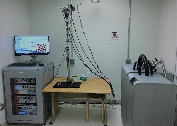
A state-of-the-art multifunctional low-temperature high-magnetic field scanning probe microscopy (LTHM-SPM) system was installed in NCMN-SMCF recently for nanoscale science and engineering research.
This LTHM-SPM is capable of characterizing spatially resolved conductivity (c-AFM), magnetic force (MFM), piezoresponse (PFM), and topography (AFM) down to the nanoscale.
The unique capabilities of the LTHM-SPM system are imaging various physical properties over a wide temperature range (4 -300 K), and magnetic field range (0-9 T). It will be a powerful tool for materials investigations.
#2
Bruker Dimension ICON Atomic Force Microscope
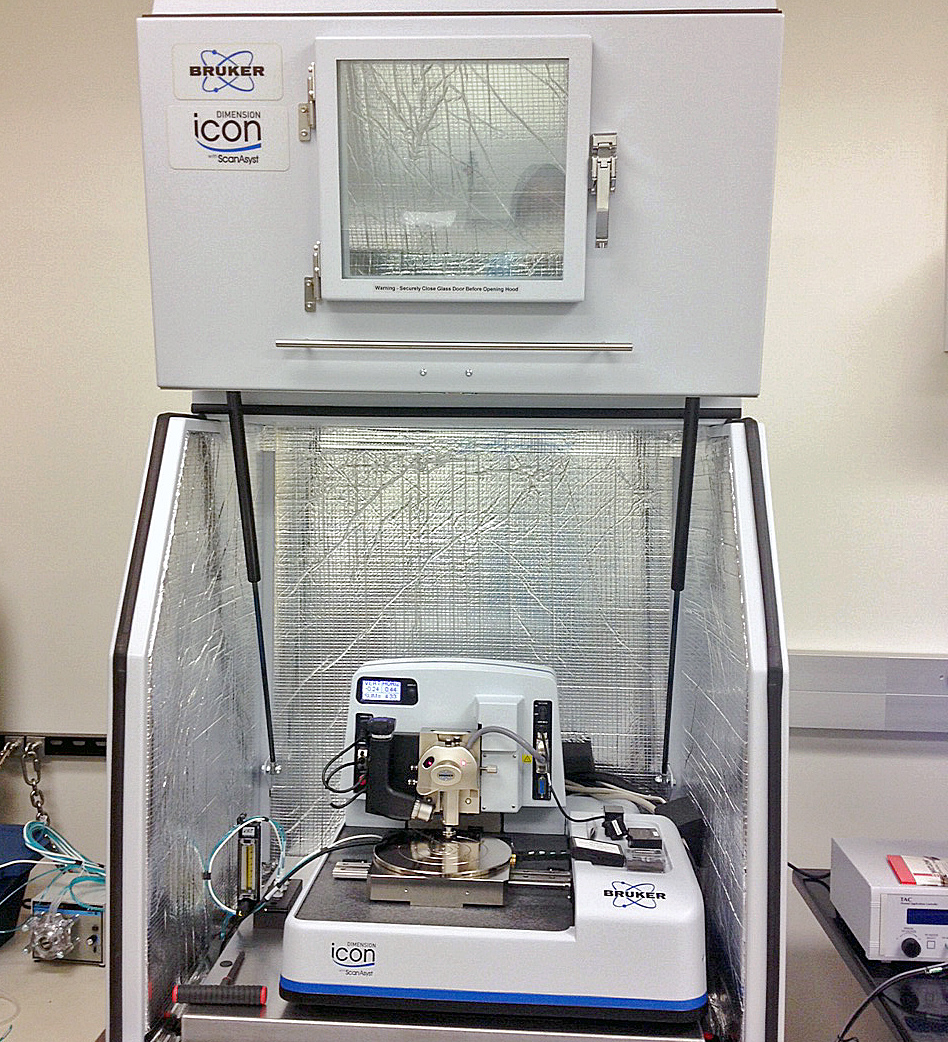
Bruker Dimension Icon® Atomic Force Microscope is equipped with ScanAsyst® automatic image optimization mode based on PeakForce Tapping technology, which enables users to obtain consistent high-quality results more easier and faster. This system is capable of many SPM applications (contact mode AFM, tapping mode AFM, ScanAsyst peakforce tapping mode, AFM in fluid, Phase imaging, piezoresponse, MFM, KPFM, and many others.) The following unique new capabilities will broaden our current SPM applications:
Material Mapping
The Icon SPM supports PeakForce QNM® Imaging Mode, enabling researchers to map and distinguish quantitatively between nanomechanical properties while simultaneously imaging sample topography at high resolution. This technology operates over an extremely wide range (1MPa to 50GPa for modulus and 10pN to 10μN for adhesion) to characterize a large variety of sample types.
Electrical Characterization
Carry out electrical characterization at the nanoscale with greater sensitivity and dynamic range using exclusive PeakForce TUNA & PeakForce KPFM modules.
Key capabilities:
- Conductivity mapping on the most delicate sample: charges, charge distribution, diffusions, surface potential distribution
- Correlated quantitative nanomechanical properties (modulus & adhesion)
- Information for rational nanostructure optimization – ID components & their distribution.
Nanomanipulation
Perform indentation and lithography at the nanometer and molecular scales. The Icon’s XYZ closed-loop scanner provides precise probe positioning with no piezo creep and extremely low noise for the best positioning of any available nanomanipulation system.
Heating and Cooling
Execute temperature control and thermal analysis on samples from 25°C to 200°C while scanning in some SPM modes.
Imaging Modes and Capabilities
- Contact Mode AFM
- TappingMode AFM
- PeakForce Tapping
- ScanAsyst® – automatic image optimization mode
- PhaseImaging
- LiftMode
- Torsional Resonance Mode (TRmode)
- Magnetic Force Microscopy (MFM)
- Electrostatic Force Microscopy (EFM)
- Lateral Force Microscopy (LFM)
- Piezo Response (PFM)
- Scanning Tunneling Microscopy (STM)
- AFM in Fluid
- Force curve
- Nano-Indentation
- Nanomanipulation (Nanolithography)
- PeakForce QNM® – new sample information with nanoscale quantitative nano-mechanical mapping (Young’s modulus, surface adhesion, energy dissipation, etc.)
- PeakForce KPFM™ – New quantitative, highest resolution workfunction measurements.
- PeakForce TUNA™ – highest resolution current mapping on fragile samples in conjunction with mechanical information.
- Sample Heating – temperature-gradient (25°C to 200°C) studies with greatest precision.
#3
DI EnviroScope Atomic Force Microscope
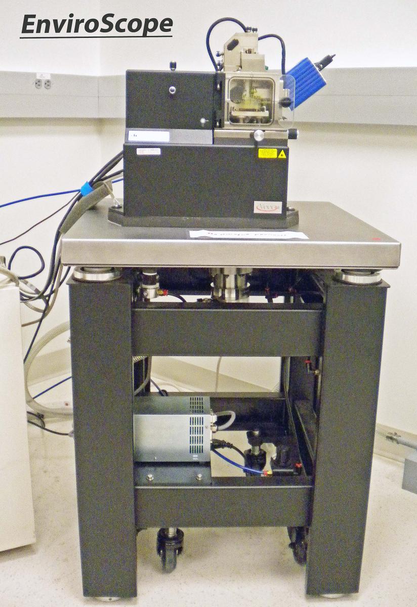
The Digital Instruments EnviroScope Atomic Force Microscope (ESCOPE) combines AFM imaging with environmental controls and hermetically sealed sample chamber to perform contact, lateral force, and TappingMode atomic force microscopy in air, vacuum, or a purged gas, as well as a heating environment. With advanced environmental capabilities, users can observe sample reactions to a variety of complex environmental conditions while scanning.
Preliminary Specifications
- NanoScope V SPM control station combines advanced analog and digital circuit designs with real-time software to provide superior multi-tasking control to provide speed, sensitivity, resolution and functionality enhancements.
- Sample stage range: 6mm XY; 14mm Z sample movement range
Sample Size: 30mm X-Y, 12mm Z
Scan Size: horizontal imaging area of 90-micron X-Y nominal maximum and a vertical range of 5-micro nominal maximum. - Optics: Improved on-axis video optics with 0.5mm field of view
- Vacuum: A Varian Turbo-V70 vacuum pump down time can be as quick as 10 minutes, depending on ESCOPE chamber cleanliness, with high vacuum capability to 10-5 Torr.
- High Temperature Heating Stage with Lakeshore Model 331 temperature controller included in the ESCOPE system. Temperature range:
Room temperature (RT) to 185 °C in ambient environment
RT to approx. 300 °C nominal at the sample surface, ~ 275 °C in vacuum.
#4
DI Nanoscope IIIa Dimension 3100 SPM system
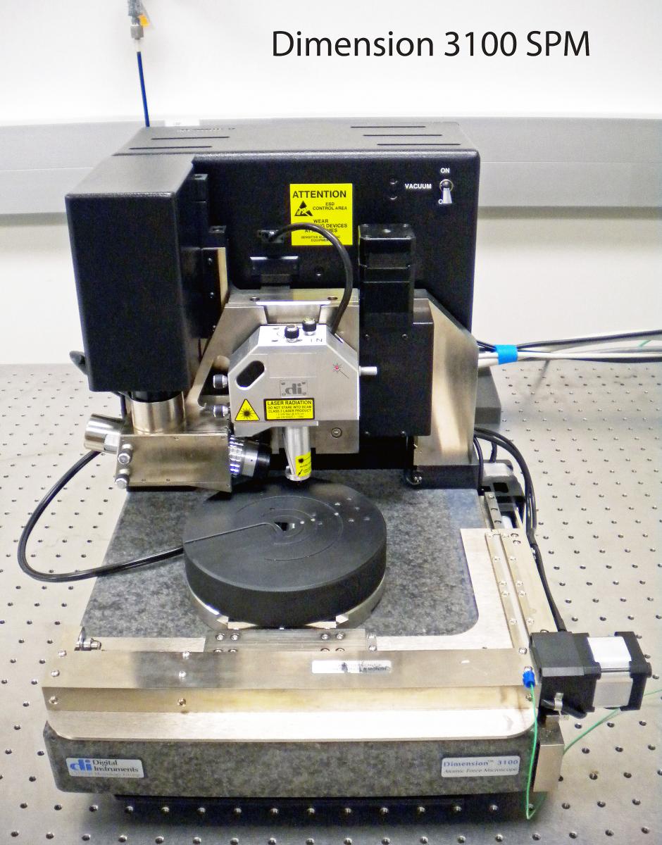
The Digital Instruments Nanoscope IIIa Dimension 3100 SPM system provides high resolution 3D images for characterization of a large variety of materials, such as nanoparticles, polymers, DNA, semiconductor thin films, magnetic media, optics and other advanced nanostructures. SPM can provide a wealth of information from topography, surface morphology, to magnetic phase or friction analysis, including line width, grain size, thin film thickness, roughness measurements, sectioning of surfaces, particle analysis, surface defects, and pattern recognition, etc.
MFM image mode can scan samples in applied external magnetic fields, which is useful for high resolution magnetic domain imaging under magnetic field. The available magnetic devices can supply magnetic fields perpendicular (-0.25 T to 0.25 T) and parallel (-0.35 T to 0.35 T) to the sample surface.
This facility contains the following equipment:
- Dimension 3100 SPM Microscopy
- NanoScope IIIa System Controller
- D3100 Microscope Electronics Box
- Dual-monitor Computer System, for data analysis, data imaging, data manipulation, and data presentation
#5
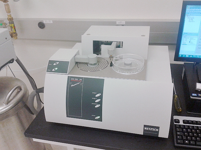
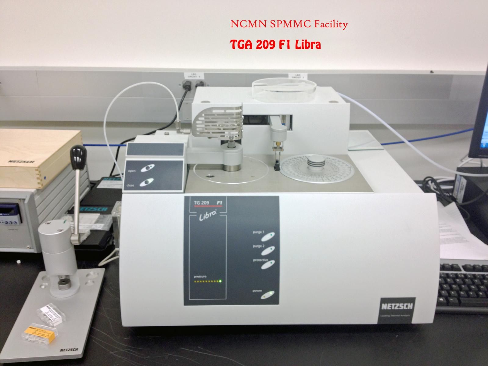
Thermal analysis systems (DSC and TGA)
The SMCF facility has two thermal analysis systems: a differential scanning calorimeter (DSC 204 F1 Phoenix) and a thermogravimetry analysis system (TGA 209 F1 Libra). Both systems operate through a large temperature range -175°C to 700°C for the DSC and 25°C to 1100°C for the TGA. These systems allow users to study and measure various thermal properties of materials such as; glass-transition temperatures, melting temperatures, melting enthalpy, crystallization temperatures, crystallization enthalpy, transition enthalpies, phase transformations, phase diagrams and other thermal properties.
two horz pictures
#6
Olympus BX51 polarizing microscope
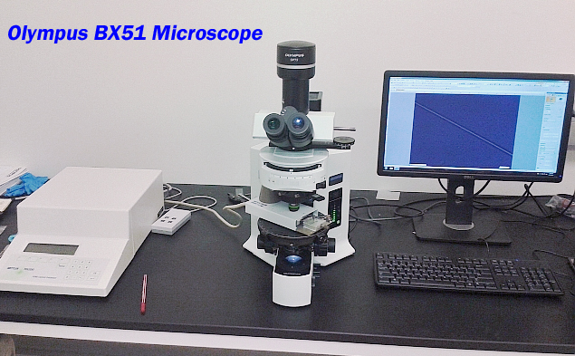
The SMCF houses an Olympus BX51 optical microscope, which includes polarizing microscope capabilities for sample viewing, and image analysis in transmission and reflection modes. In addition, the thermal behavior of a sample can be observed under the microscope using a Mettler Toledo FP900 thermal system equipped with a FP 82 hot stage with a temperature range of room temperature to 375° C.
#7
Tukon 2500 Knoop and Vickers tester
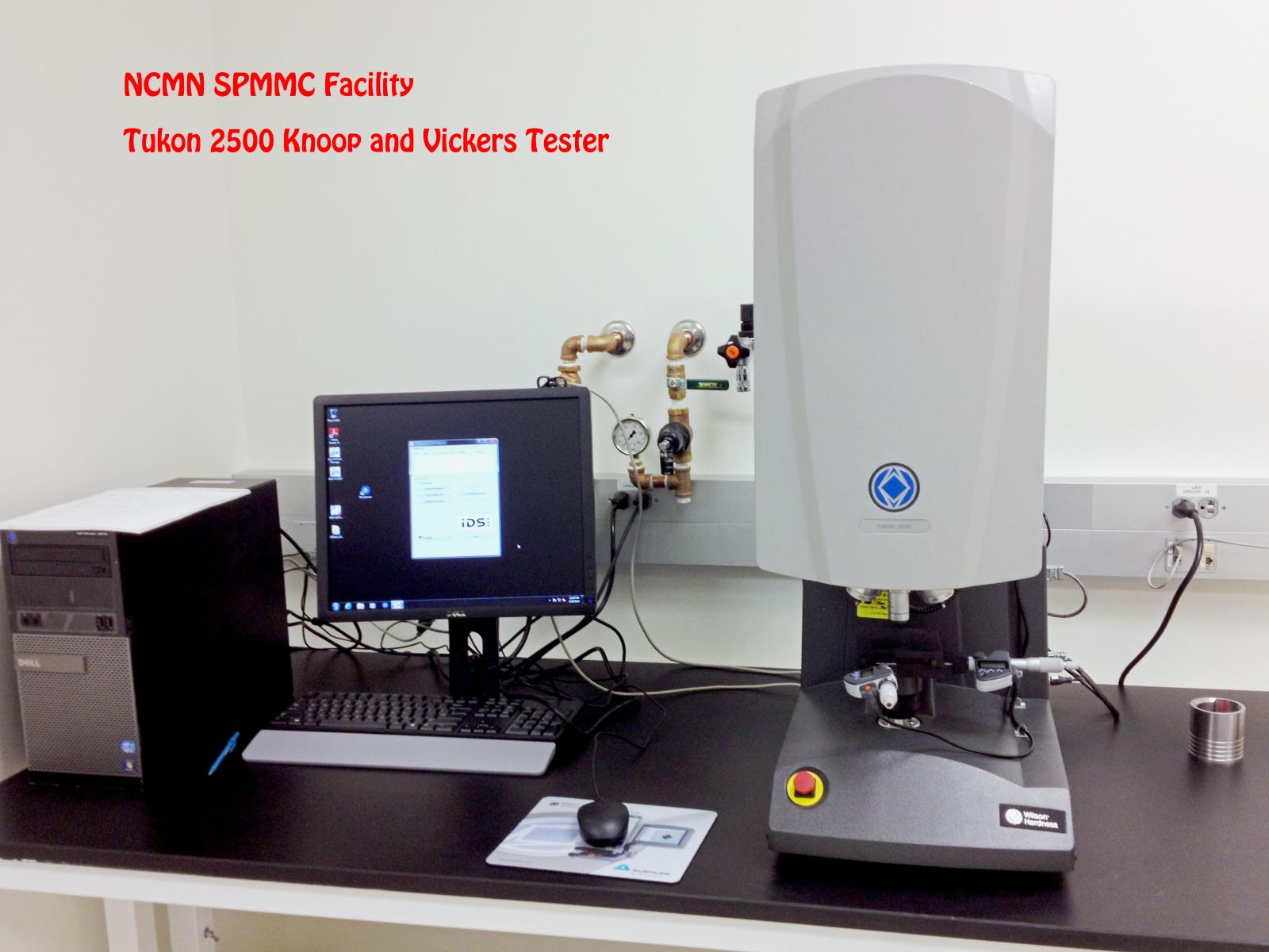
Vickers/Knoop Hardness Tester measures mechanical hardness of materials. The Vickers/ Knoop microhardness test is used particularly for small parts, very brittle materials or thin sheets, where only a small indentation may be made for testing purposes. The test force range: 10 g to 1000g. Hardness testing involves using a known load and a known indenter shape which is then pressed into a material. The depth of penetration of the indenter is proportional to the hardeness of the material. Hardness data can be used to infer other mechanical properties of material.
#8
ThermoFisher K-Alpha XPS/UPS Photoelectron Spectrometer
Please contact Dr. Steve Michalski (smichalski@unl.edu) for further information and training.
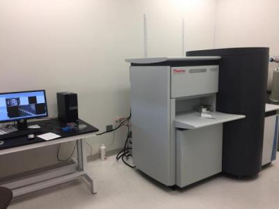
X-ray photoelectron spectroscopy (XPS) is a surface analytical technique, which is based upon the photoelectric effect and measures the elemental composition, empirical formula, and chemical state of the elements within a material. XPS spectra are obtained by irradiating a solid surface with a beam of X-rays (Al Ka with an energy of 1486.6 eV) while simultaneously measuring the kinetic energy of photoelectrons that are emitted from the top 1-10 nm of the material being analyzed. Since the core-level XPS peaks for different elements appear at particular characteristic energies, the energies and intensities of the XPS peaks enable the identification and quantification of all elements from the surface (except hydrogen). Similarly, the chemical shifts and appearance of other special features, for example satellite and plasmon-loss peaks, in the XPS spectra are useful for chemical state analysis.
XPS has various scanning options: (i) Point scan: the spot size of the x-rays can be varied from 30 to 400 mm in 5 mm steps; (ii) Line and area scans are also possible with a maximum spatial resolution of 30 mm or better; (iii) K-alpha+ XPS is also capable of mapping the surface with a maximum spatial resolution of 30 mm or better and this is useful in understanding the elemental distribution across a surface.
A few other key features of the K-alpha+ XPS are also given below:
Charge Compensation: If the surface of a material is electrically insulating, then the emission of photoelectrons causes a positive charge to accumulate at the surface. This causes the XPS peaks to shift to high binding energies. The charge on the surface can be neutralized by replenishing electrons from an Ar-ion flood source during the measurement.
Depth Profiling: XPS also has an Ar ion beam for depth-profiling measurements (beam energy: 0.1 to 4 keV, current £ 4 mA). This is helpful in etching away the surface contamination and also to investigate subsurface information. Combining a sequence of ion-gun etch cycles with XPS analyses provides quantified information as a function of layer thickness.
Angle-resolved XPS (ARXPS): We also have a sample holder that can be tilted for performing ARXPS. ARXPS enables electron detection from different depths by varying the emission angle at which the electrons are collected. Such measurements are non-destructive and can be applied to films that are too thin to be analyzed by conventional depth-profiling techniques or films that are irretrievably damaged by sputtering (e.g., polymers).
Ultraviolet Photoelectron Spectroscopy(UPS) operates on the same principle as XPS, but ultraviolet (UV) radiation is used to induce the photoelectric effect. UV photons are produced using a gas discharge lamp, typically filled with helium and have energies of 21.2eV (He I) and 40.8eV (He II). As lower energy photons are used, spectral acquisition is limited to the valence-band region. UPS can precisely measure the Fermi edge, density of states in the valence band, and electronic work function of a material being investigated.
XPS/UPS system is user friendly and Avantage software allows complete instrument control, data acquisition, and data processing. Samples/specimens should be in solid forms such as thin films, powders, pellets, fibers, etc.
#9
Other equipment
- Buehler ISOMet 1000 Precision Saw
The IsoMet 1000 Precision Saw offers increased speed, load, and a 7-inch diamond blade capacity that enables a wide variety of advance materials to be cut quickly and with low deformation. - Buehler MiniMet 1000 Grinder-polisher
The MiniMet 1000 Grinder-polisher is a sample preparation system with adjustable speed and high pressure capability that quickly prepares materials (such as ceramics, composites, and metals) for cross-sectional analysis.
- Sartorius Cubis MSU2.7S-000-DM Microbalance
Microbalance with readability of 0.0001 mg is high-resolution measuring instrument used for measuring sample up to 2.1g weighing capacity.